Specifications and Features
| Chipset | X99 | X79 |
| Socket | 2011-3 | 2011 |
| Memory Channels | 4/1 DDR4 | 4/1 DDR3 |
| USB 3.0 Inputs | 6 | 0 |
| Sata 6 Inputs | 10 | 2 |
| CPU Overclocking | Yes | Yes |
| Memory Overclocking | Yes | Yes |
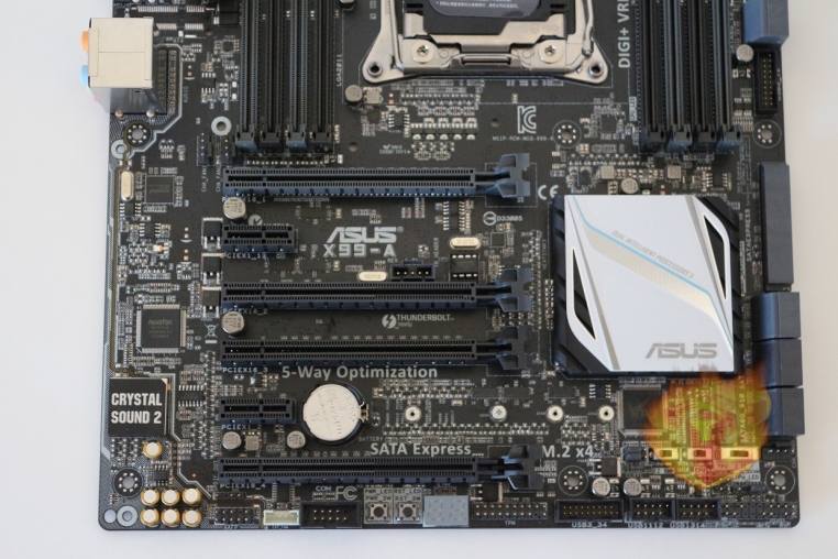
Haswell-E brings a brand new and long awaited refresh to the popular enthusiast X79 platform from 2011 with the X99 Chipset. Some notable features include 6 USB 3.0 inputs, 10 SATA 6GB/s inputs, 32 GB/s M.2 support, thunderbolt support, and of course 8 DDR4 DIMM slots.
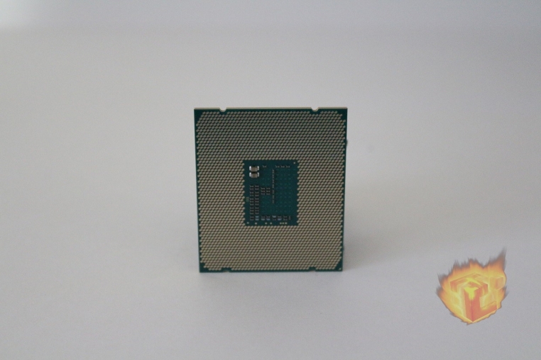
With Intel’s 5960X every feature is included and almost nothing is missing, what really stands out breaks the boundary between something like an i7-4790k is the PCI-E lane support, the massive 2011-3 socket, and DDR4. Nevertheless, If on-board graphics are a necessity please look elsewhere, none of Intel’s enthusiast series “E” processors contain any form of on-board graphics and the 5960X is no exception.
With support for 40 lane CPU the 5960X is capable of 4-way crossfire or SLI and depending on motherboard specifications speeds of 16x can be reached on the PCI-E for up to 3 cards. What this mean for multi graphics cards users is more bandwidth for each card to communicate with the CPU and chipset, this is analogous to adding more lanes to a highway to alleviate heavy traffic. The 4th slot, if supported, only has 8x speed which may cause some performance degradation on paper but may not even be an issue for something like a gaming set up. Testing on 3 and 4 graphics cards with different lane configurations is underway for a future article.
 |
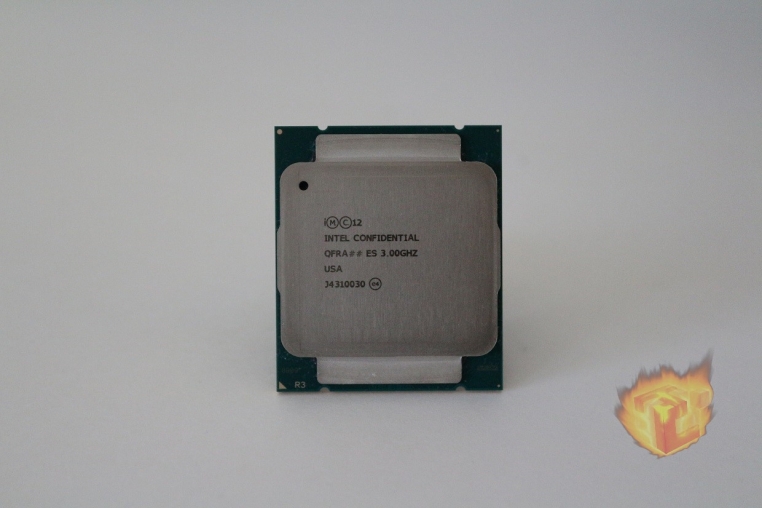 |
One major thing to not that may confuse many users is that the X99 2011-3 sockets is NOT the same as the X79 2011 socket, a 5960X will not work on a X79 motherboard. The socket still look visually similar to its X79 counterpart with a large and bulky socket with pins that are visible with a CPU placed in the socket unlike the smaller Z97 variants. The giant surface area of all X99 CPU allows for more heat transfer between the CPU and the heat sink and thanks to Haswell-E’s soldered on die one can expect this monster of a CPU to run extra cool. Unlike previous iterations of CPU where Intel used, often low quality, thermal paste the Haswell-E uses solder between the die and chip so de-lidding this CPU is not an option when looking for extra thermal headroom. Like all Intel CPUs, the physical feel and look of this heavy piece of 22nm silicon is a testament of modern technology.
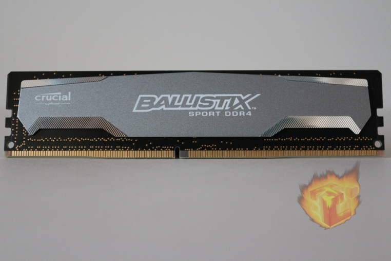
DDR4, perhaps the most notable feature of this release still has many unanswered questions as factories ramp up DDR4 module production and the cost drops. There is no doubt that DDR4 will overtake DDR3 as the main form of memory once DDR4 platforms become more mainstream. With the 5960X Intel took a gamble but not using such new technology as a lot could have gone wrong, unfortunately with new technology comes high upfront costs. This article is not a DDR4 review but in essence the main technical difference between DDR4 and DDR3 is lower voltage and higher speeds, for example, your average entry DDR4 DIMM is capable of 2400MHz at 1.2V without any overclock.
Haswell-E Architecture

Haswell and Haswell-E is considered a “tock” in Intel’s Tick-Tock release cycle, a tock is simply an upgrade to the existing 22nm architecture found in Ivy Bridge-E. Notable upgrades between the 2 architectures include 8% better vector processing, 6% faster single threaded performance, 6% faster multi-threaded performance and a 6% increase in sequential CPU performance. All the differences between Ivy Birdge and Haswell are of course design upgrades and not actual real world values between the two, refer to the benchmarking section of this article for measurable results. Visually,the Haswell-E architecture looks almost identical to Ivy Bridge -E with the major exception of 8 cores instead of 6. Haswell-E contains a transistor count of 2.6 Billion compared to Ivy Birdge-E’s 1.86 Billion however, the die size for Haswell-E is bigger at 17.6mm x 20.2mm compared to 15mm x 17.1mm and of course the 5MB upgrade of shared cache between the two generations. What does this all add up to? It shows that Moore’s law still hols through and that on paper Haswell-E should provide a significant performance boost over Ivy Bridge-E.

You must be logged in to post a comment.