![]()
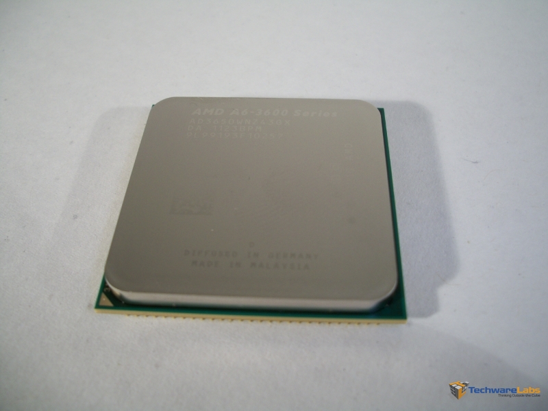
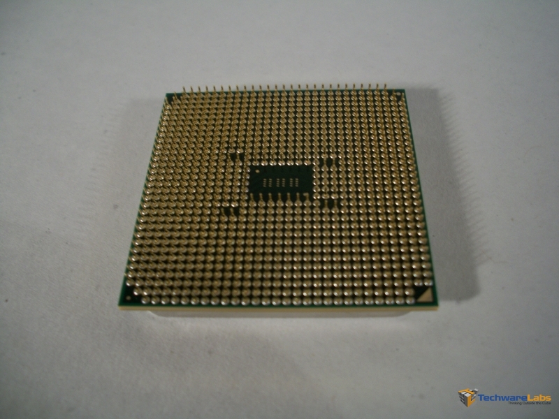
An in-depth look at the AMD A6-3650
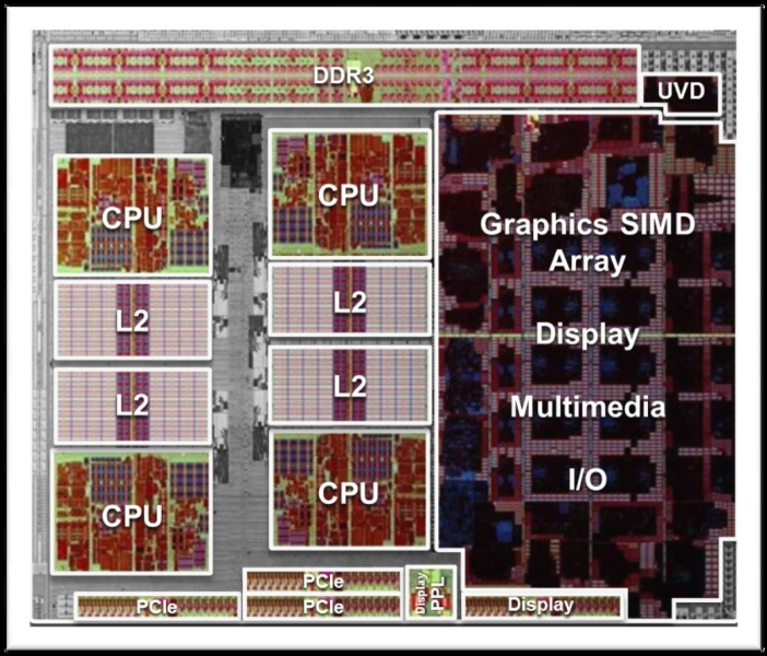
To get a better idea behind the architecture of this APU it will need to be dissected a bit for you. ‘Llano’ processors are made on a 32nm node with a chip die-size of 228 mm, which is very comparable to SandyBridge, the APU has roughly 1 Billion transistors.
 |
 |
It has three primary elements merged into the APU, the Northbridge, the CPU and the GPU. Intel places more focus on raw CPU performance, AMD places more focus on the multi-media experience, thus the GPU.
There is more to be found inside the APU than what I have already mentioned. There is a DDR3 memory controller, Unified Video Decoder core logic, the Northbridge, a PCI Express interface, and last, but not least a DDI interface to output to digital monitors.

[…] high load operations like your video transcoding, more cores = faster encoding, here is a review — AMD A6-3650 APU/Processor | TechwareLabs. BASILISK — HOME PC — Reply With Quote + Reply to Thread […]
[…] Reviews goes inside the BitFenix Shinobi Computer CaseTechwareLabs shares its thoughts on the AMD A6-3650 APU/ProcessorKitGuru gives a listen to some KWorld Classic C40 Computer Speakers bit-tech takes on EYE: Divine […]
[…] story at Techware Labs. Posted in: Affiliate […]
[…] AMD A6-3650 APU/Processor Review @ TechwareLabs […]
[…] AMD A6-3650 APU/Processor Review @ […]